Scientists are striving to discover new semiconductor materials that can increase the efficiency of solar cells and other electronic devices. However, the pace of innovation is bottlenecked by the speed at which researchers can manually measure key material properties.
A fully autonomous robotic system developed by MIT researchers was able to speed things up.
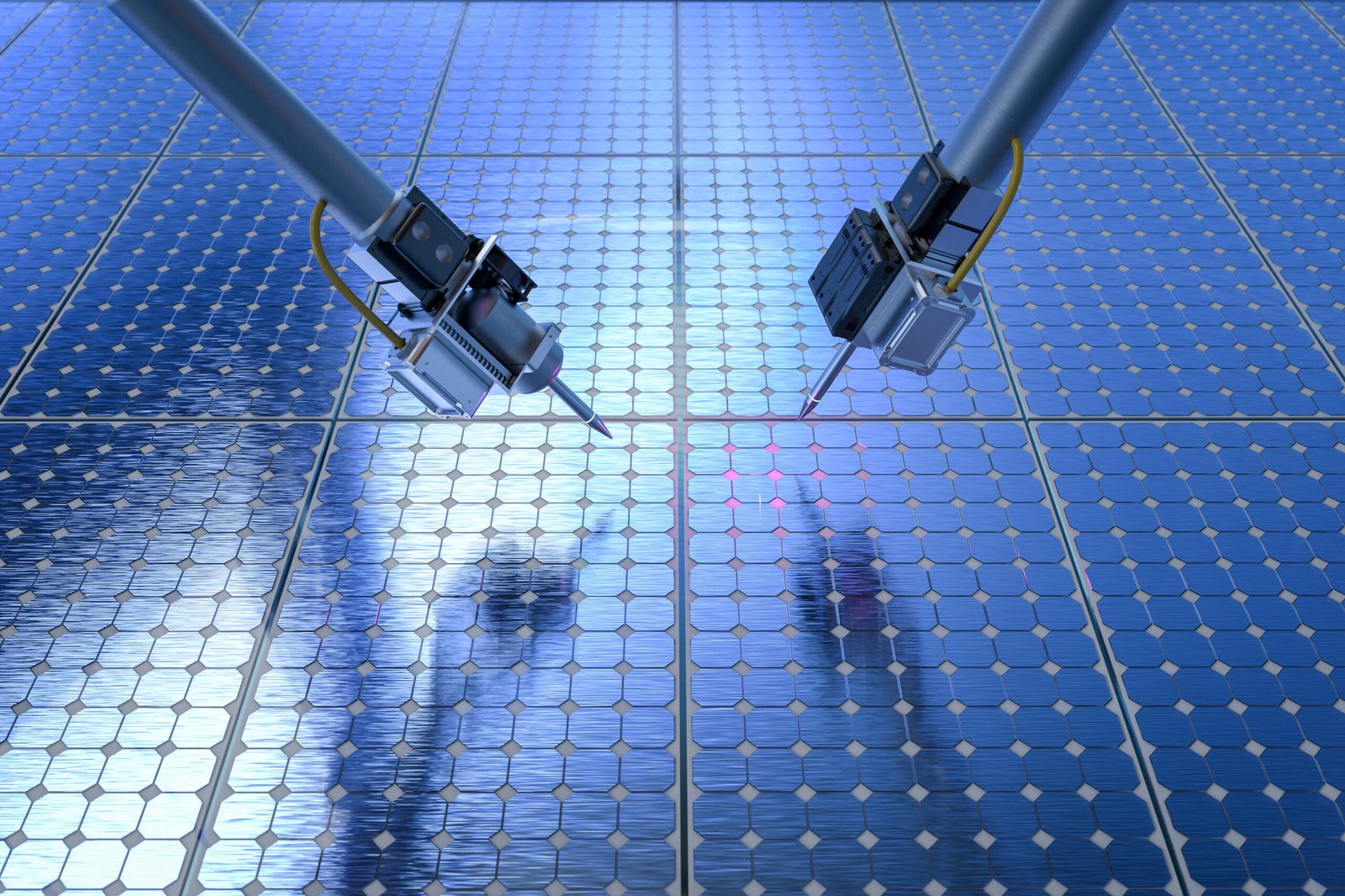
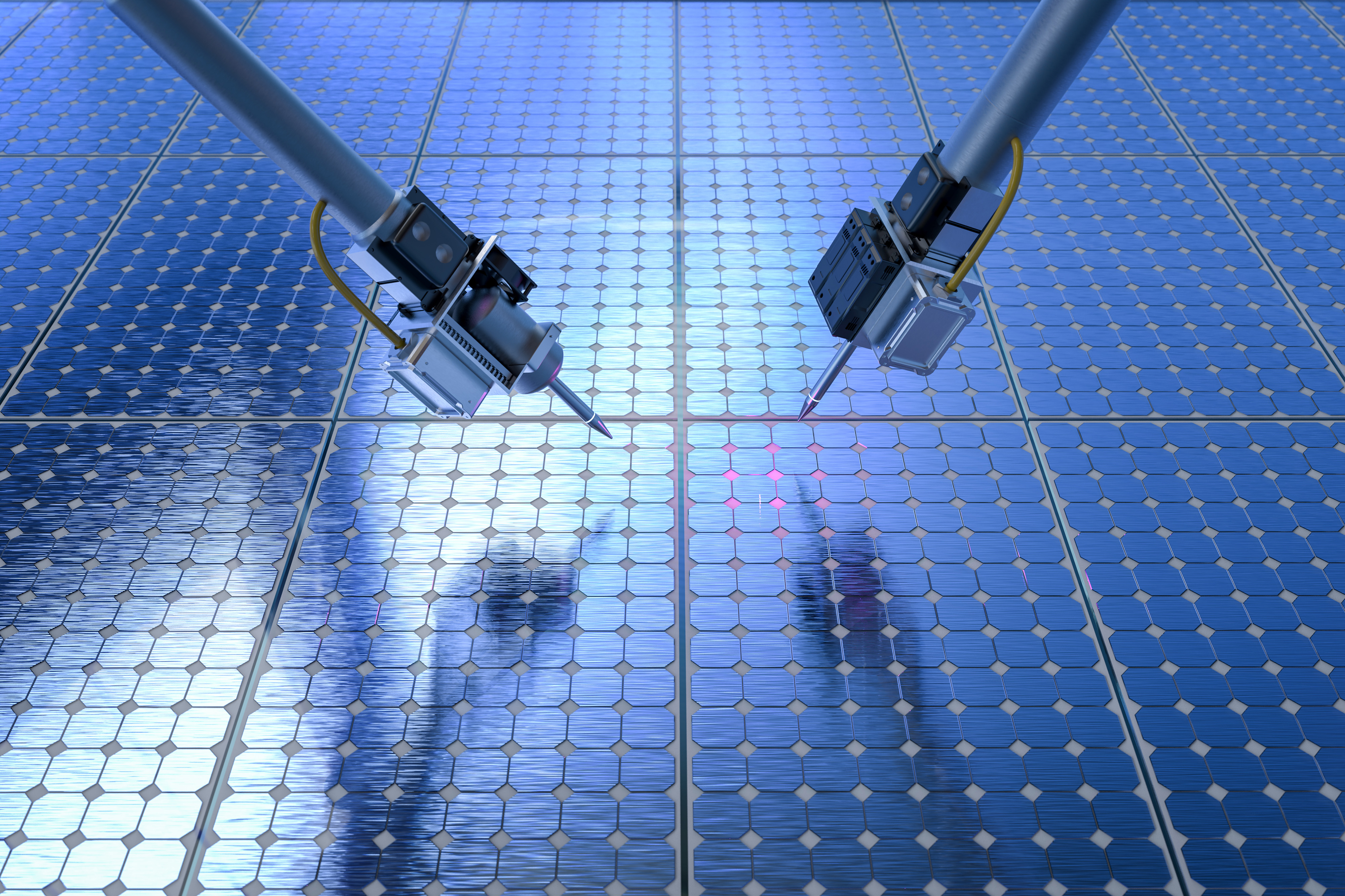
Their systems utilize robotic probes to measure important electrical properties known as photoconductivity. This is the electrical responsiveness of the material to the presence of light.
Researchers inject materials science domain knowledge from human experts who guide robotic decision-making into machine learning models. This allows the robot to use the probe to identify the best location to contact the material, providing the most information about its photoconductivity, but specialized planning procedures will find the fastest way to move between contacts.
During the 24-hour testing, the fully autonomous robotic probe took over 125 unique measurements per hour, with more accuracy and reliability than other artificial intelligence-based methods.
By dramatically increasing the speed at which scientists can characterize important properties of new semiconductor materials, this method could facilitate the development of solar panels that generate more power.
“I think this paper is very exciting as it provides a pathway for autonomous contact-based characterization methods. Not all important properties of the material can be measured in a contactless manner. If you need to contact the sample, you want to maximize the amount of information you have acquired.
His co-authors include authors Alexander (Alex) Siemen, a graduate student. Postdocs Basita Das and Kangyu Ji; Graduate student Hwang Shen. Work is coming today Advances in science.
I’ll get in touch
Since 2018, researchers at Buonassisi’s Institute have been working towards a fully autonomous material discovery laboratory. They recently focused on the discovery of a new perovskite, a class of semiconductor materials used in solar power generation, such as solar panels.
Previous research has developed techniques for rapidly synthesizing and printing unique combinations of perovskite materials. We also designed an imaging-based method to determine several important material properties.
However, photoconductivity is most accurately characterized by placing a probe on a material, illuminating the light, and measuring the electrical response.
“To ensure that the lab works as quickly and accurately as possible, we had to come up with a solution that would generate the best measurements while minimizing the time it took to perform the entire procedure,” Siemenn said.
This required the integration of machine learning, robotics and materials science into one autonomous system.
First, the robot system uses an onboard camera to capture images of slides printed with perovskite material.
Then, use computer vision to cut the image into segments. This is fed into neural network models specifically designed to incorporate domain expertise of chemists and materials scientists.
“These robots can improve the reproducibility and accuracy of our operations, but it’s important to have humans in the loop. Without a good way to implement the wealth of knowledge from these chemical experts in the robot, we cannot discover new materials,” adds Siemen.
This model uses knowledge of this domain to determine the optimal point of contact for the probe based on the sample shape and its material composition. These contact points are fed to the pass planner who finds the most efficient way for the probe to reach all points.
The adaptability of this machine learning approach is particularly important as printed samples have unique shapes, ranging from circular droplets to jellybean-like structures.
“It’s like measuring snowflakes. Getting two identical ones is difficult,” Buonassisi says.
When the pass planner finds the shortest path, it sends a signal to the robot’s motor. It operates the probe and quickly and continuously measures the measurements at each contact point.
The key to the speed of this approach is the self-monitored nature of neural network models. This model directly determines the optimal contacts in the sample image without requiring labeled training data.
Researchers also accelerated the system by strengthening path planning procedures. They found that adding a small amount of noise or randomness to the algorithm can help you find the shortest path.
“As we move into this autonomous institute era, all three of these expertise (understanding hardware building, software and materials science) need to be able to come together in the same team and innovate quickly. That’s part of the secret source here,” Buonassisi says.
Rich data, fast results
Once they built the system from scratch, researchers tested each component. Their results showed that the neural network model found better contact points with fewer computational times than the other seven AI-based methods. Furthermore, the path planning algorithm has found a more consistently shorter path planning than the other methods.
After performing a 24-hour, fully autonomous experiment with all pieces together, the robotic system performed over 3,000 unique photoconductivity measurements at speeds greater than 125 per hour.
Furthermore, the level of detail provided by this accurate measurement approach allowed researchers to identify hot spots that not only have high photoconductivity but also have degraded areas of material.
“The ability to collect such a wealth of data that can be captured at such a fast rate without the need for human guidance, will allow us to discover and develop new, high-performance semiconductors, especially for sustainability applications such as solar panels,” says Siemenn.
Researchers want to continue building on top of this robotic system as they strive to create fully autonomous labs for material discovery.
This work is supported in part by the MIT Energy Initiative, Mathworks, the Acceleration Consortium of the University of Toronto, the US Department of Energy, and the National Science Foundation, first solar, ENI.